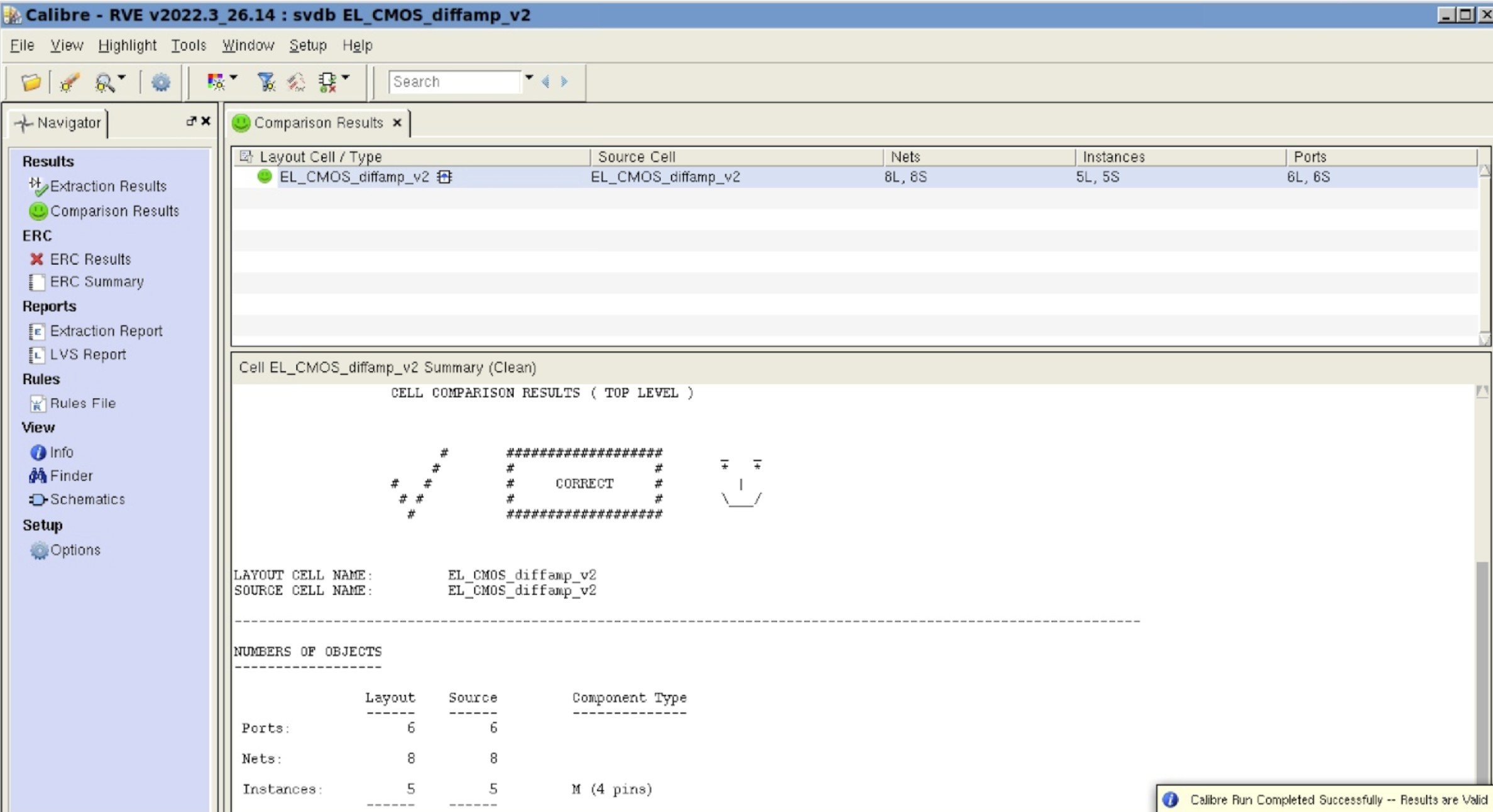
Made a differential amplifier subsection in a chip from some inverters, passgates, a code checker, and a mosfet diff amp.
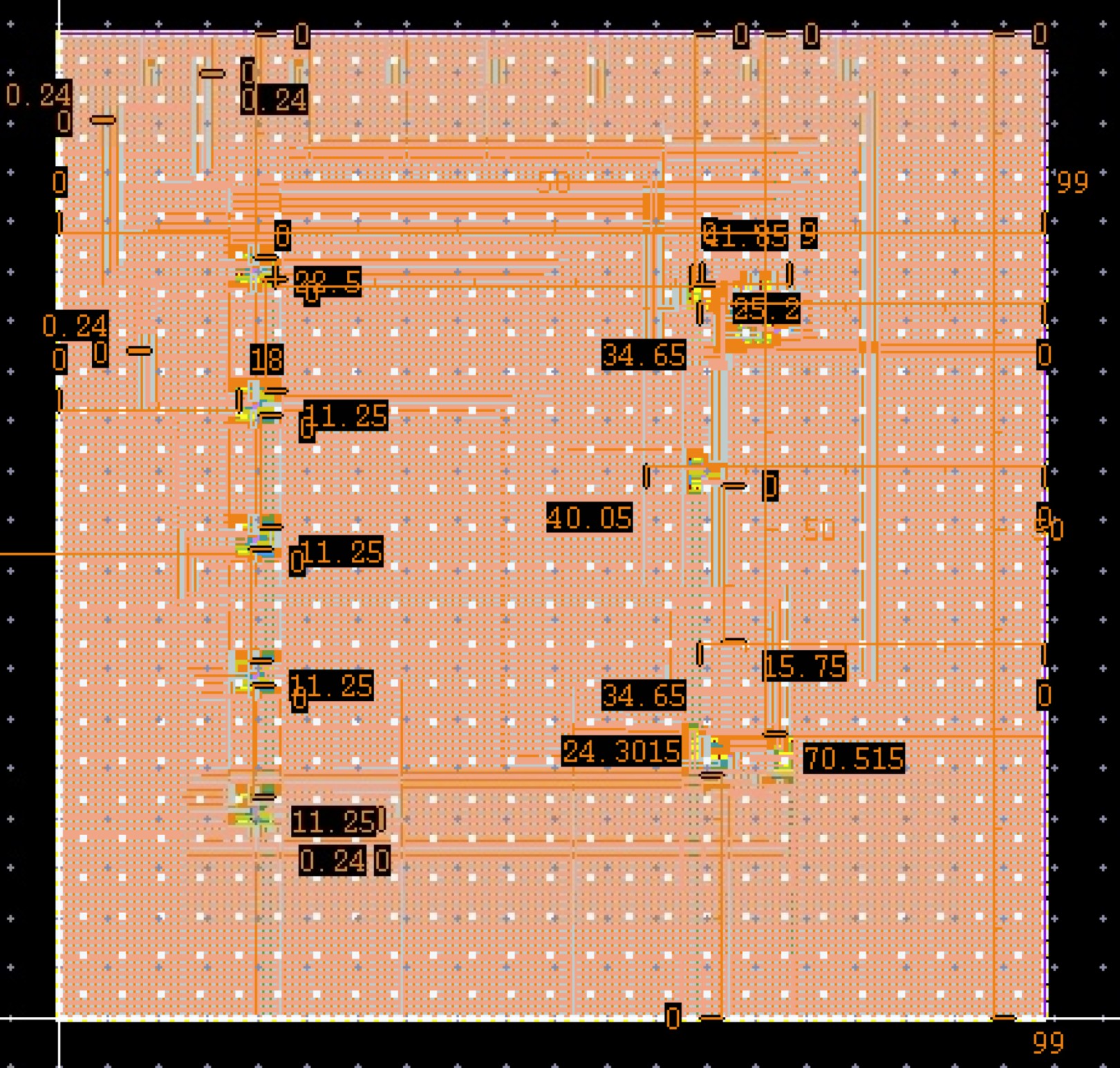
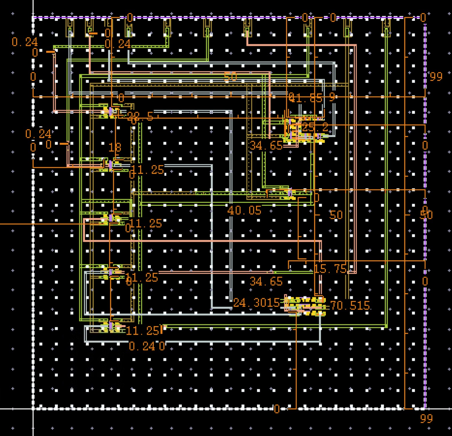
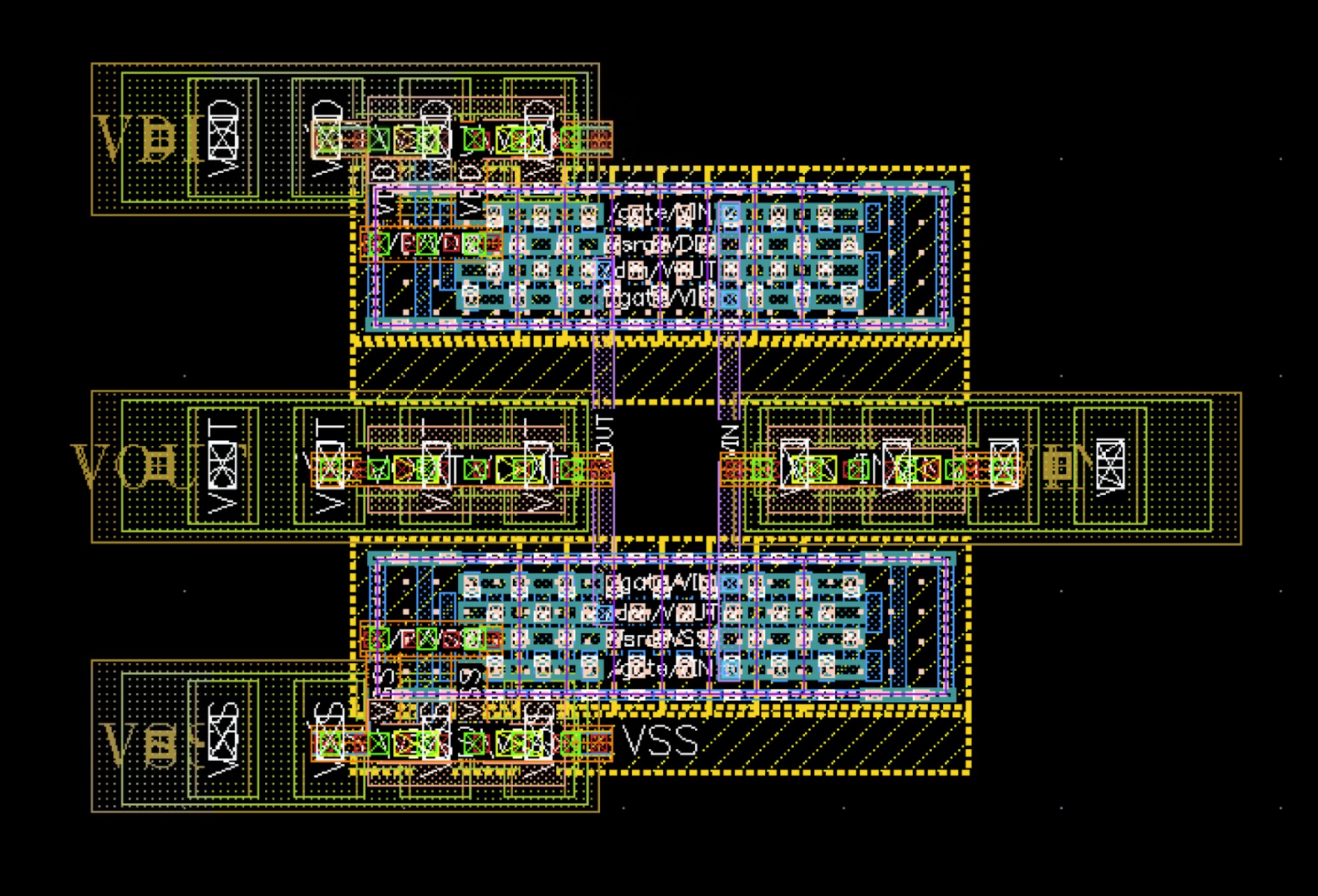
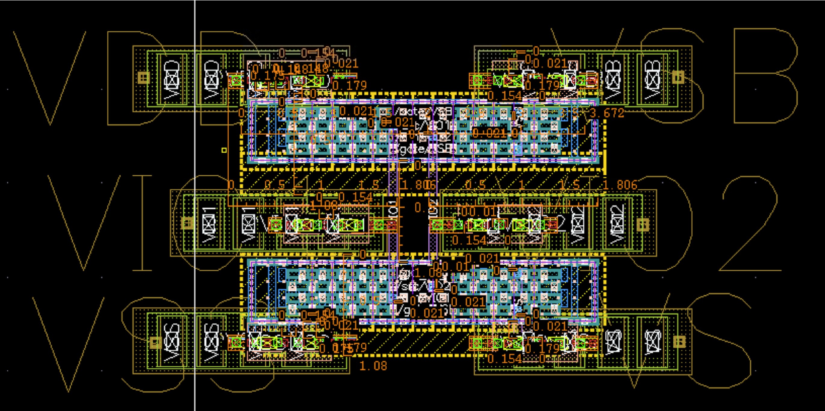
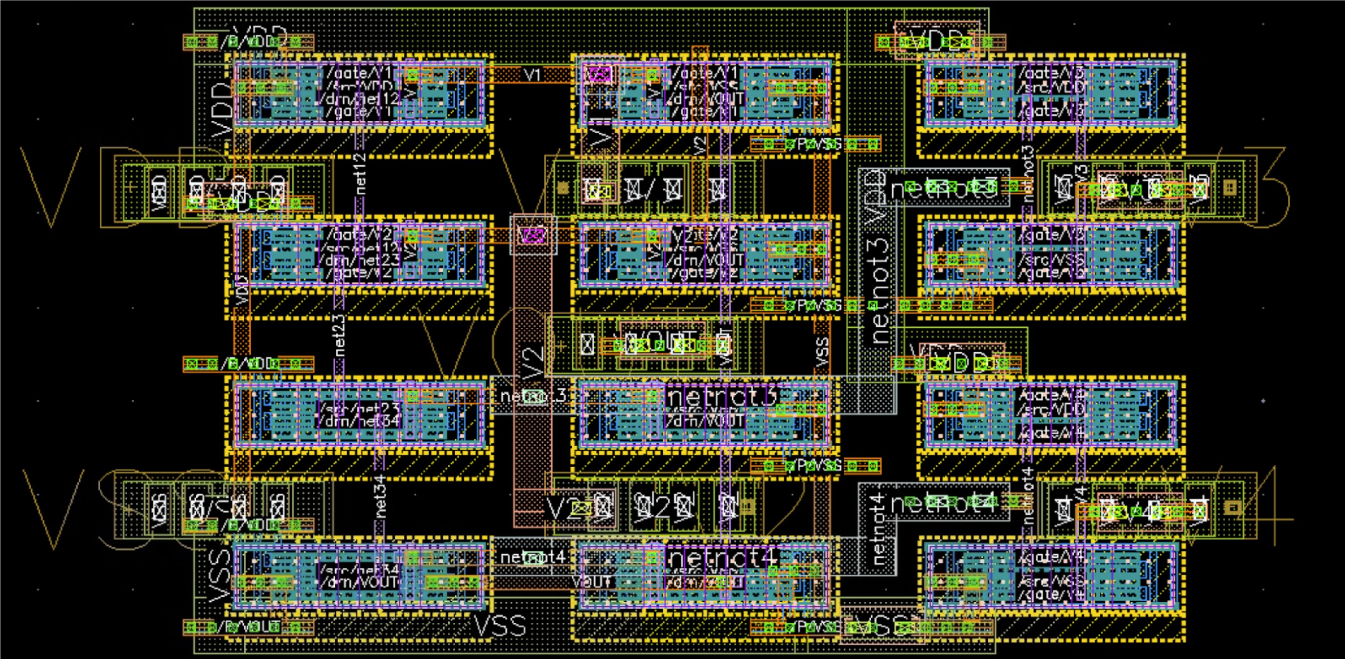
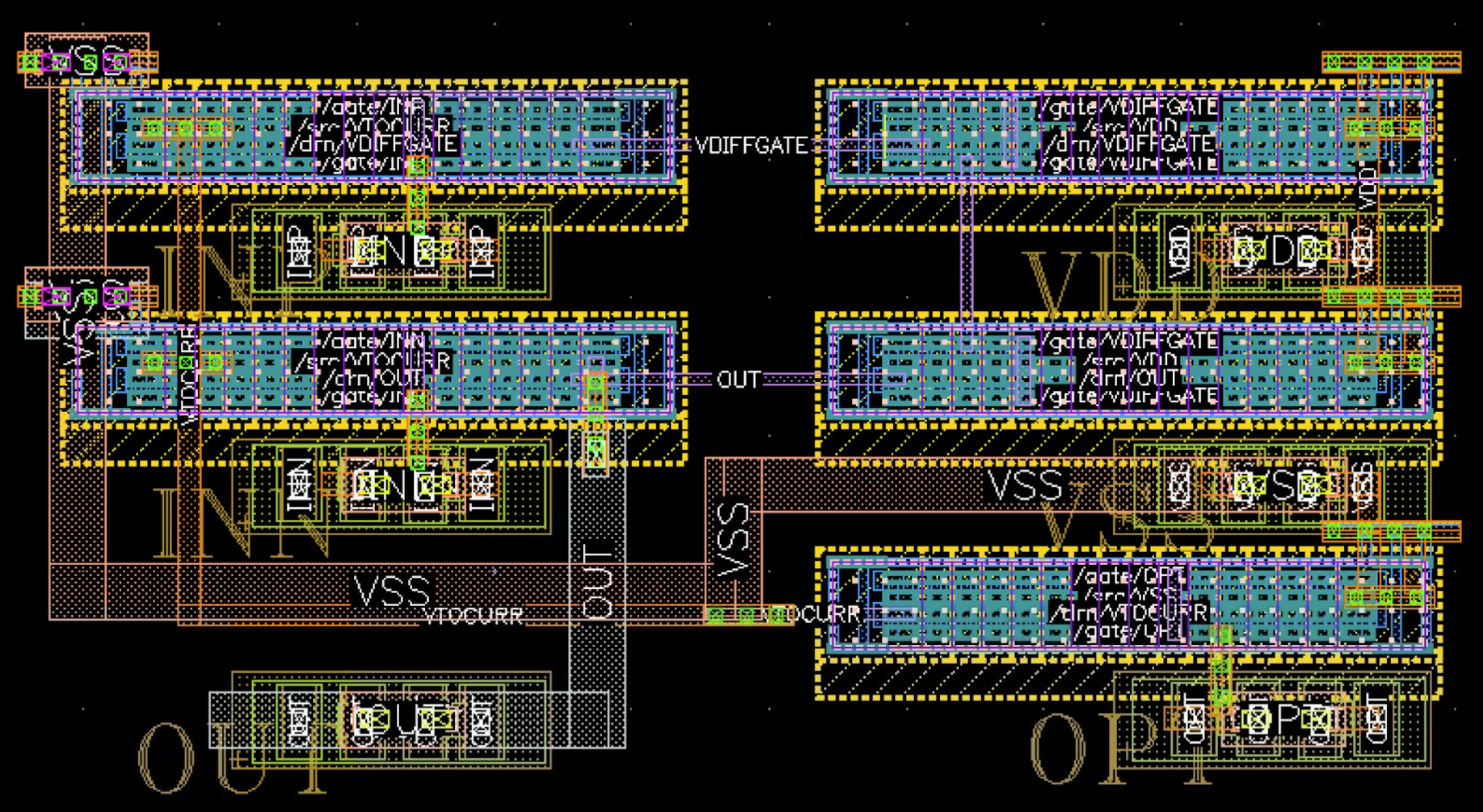
Layout of Full System
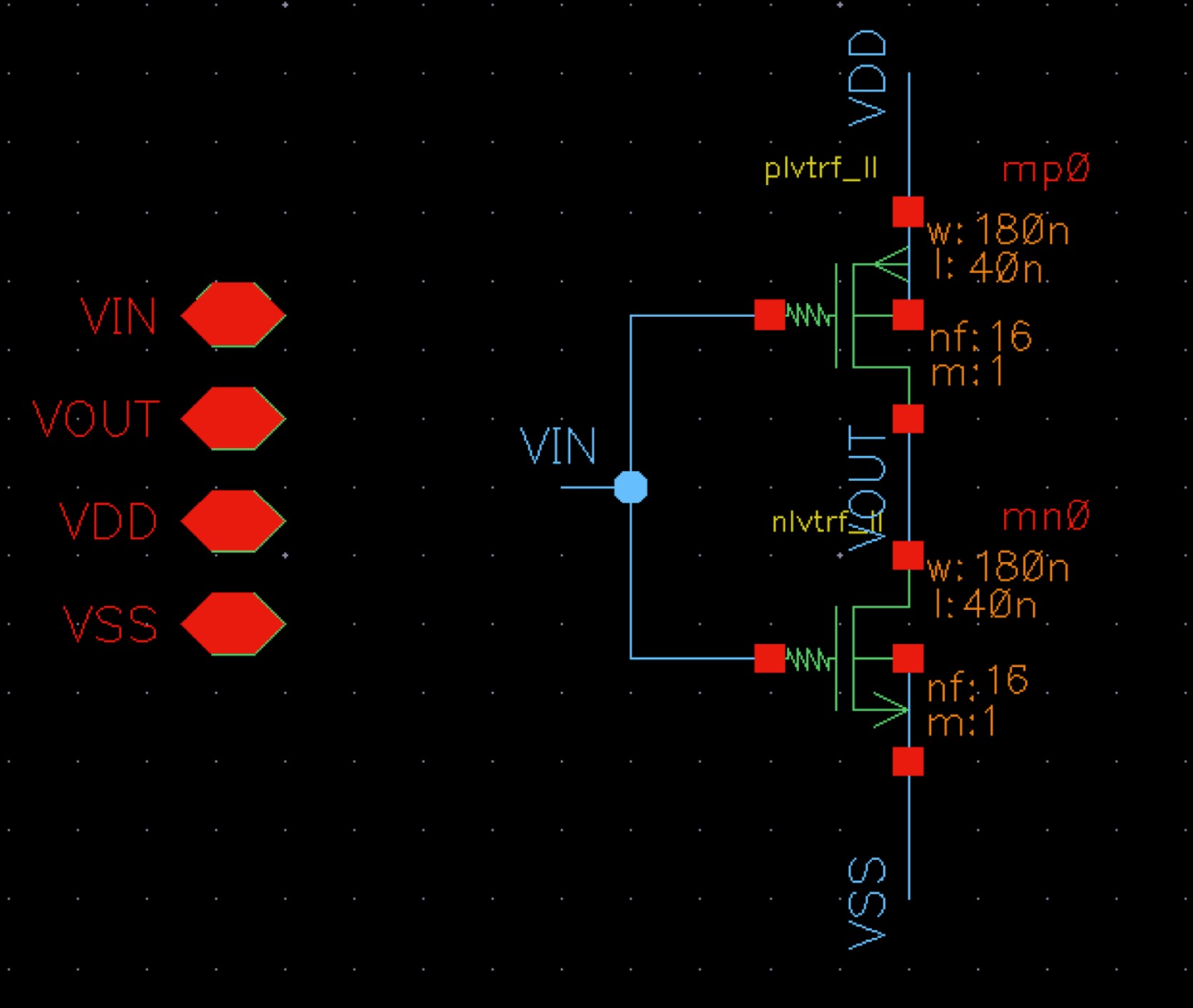
Inverter
Transistor Sizing:
- mp0: NF = 16
- mn0: NF = 16
Inverter Simulation:
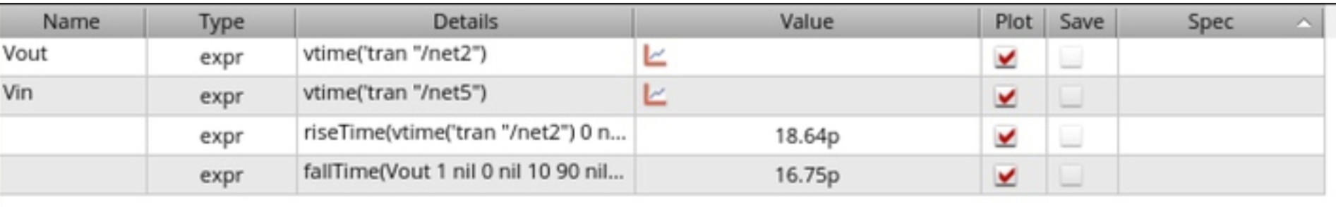
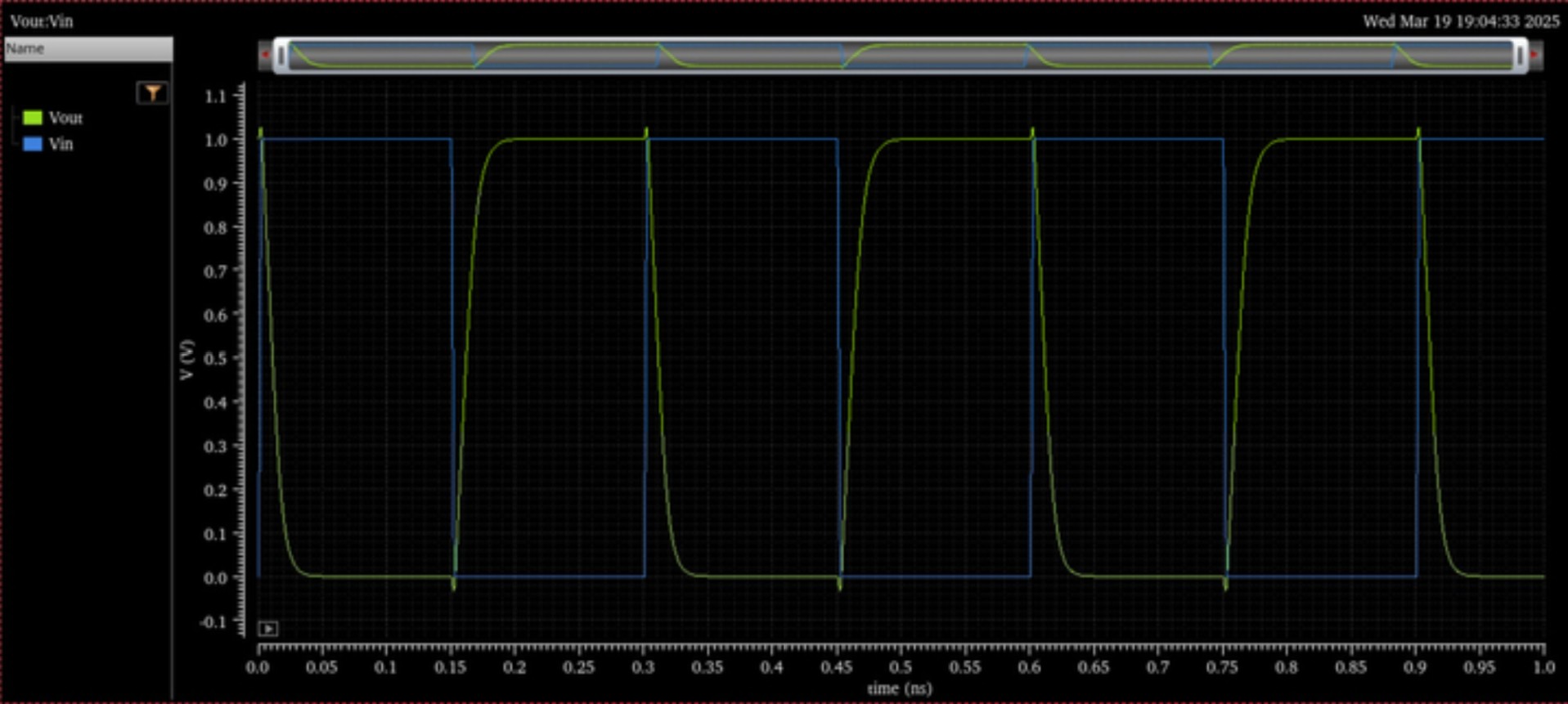
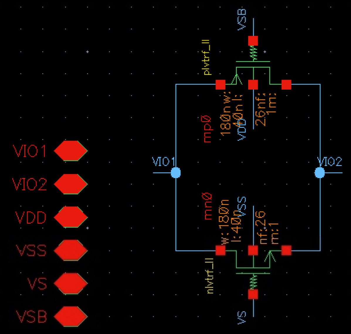
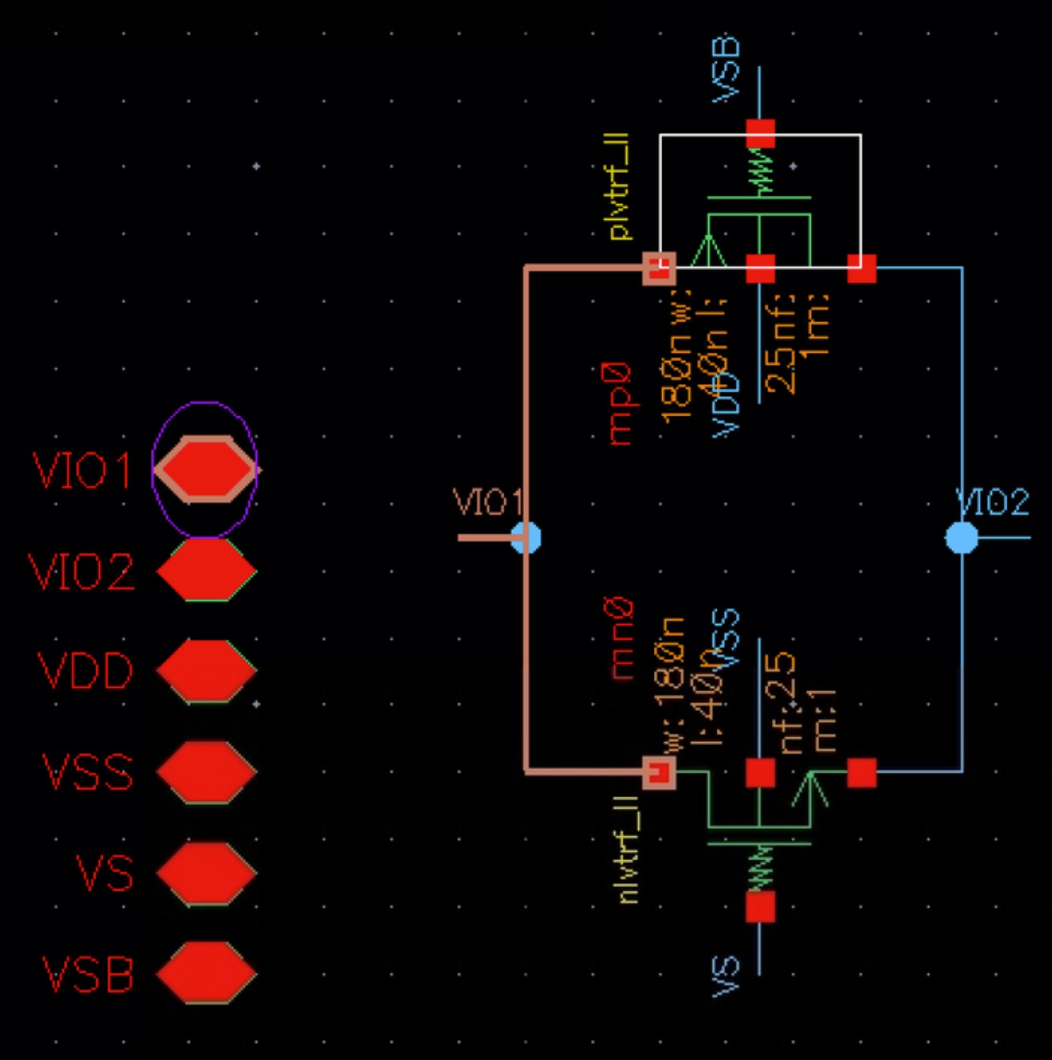
Passgate
Transistor Sizing:
- mp0: NF = 26
- mn0: NF = 26
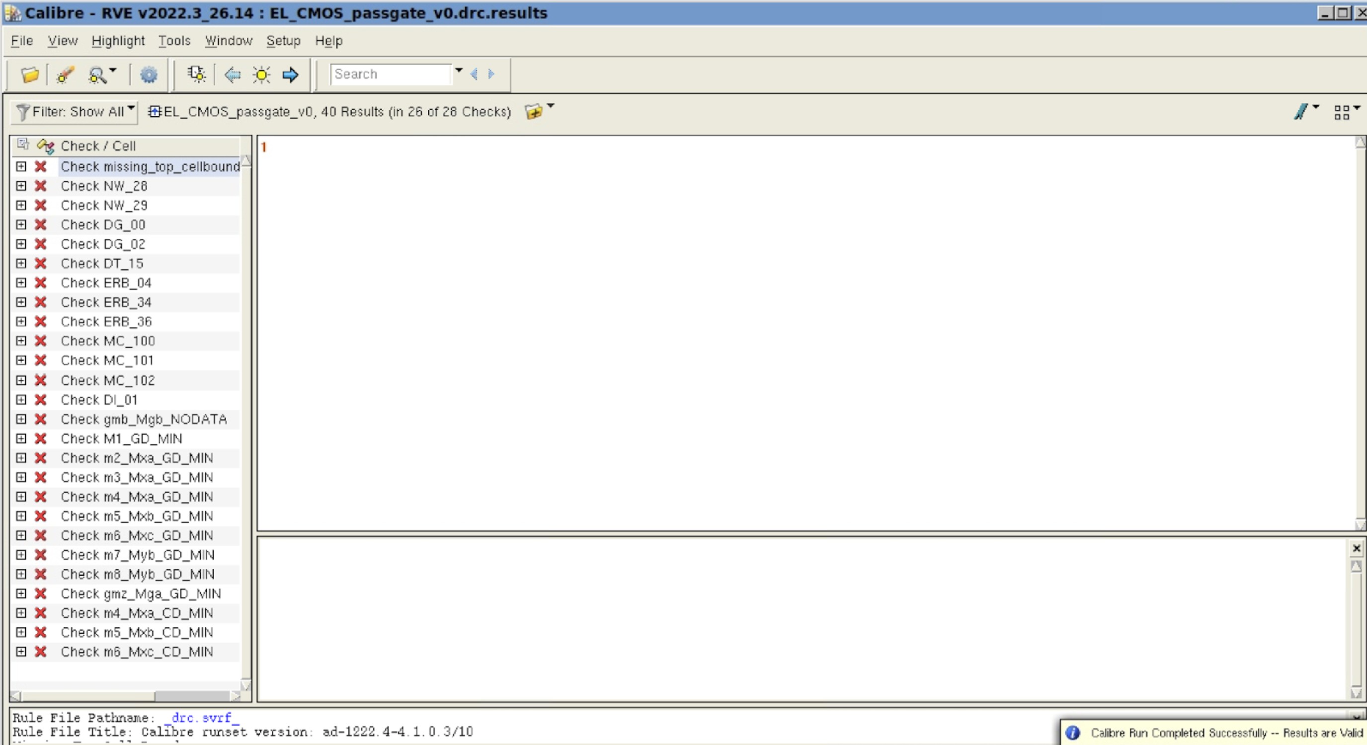
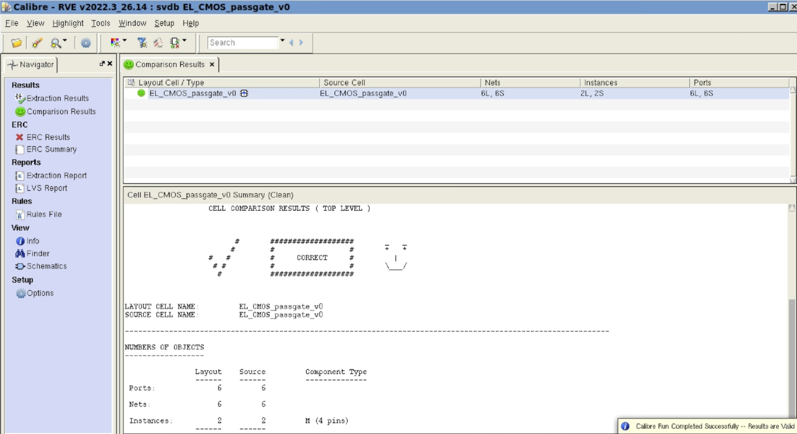
Passgate Simulation:
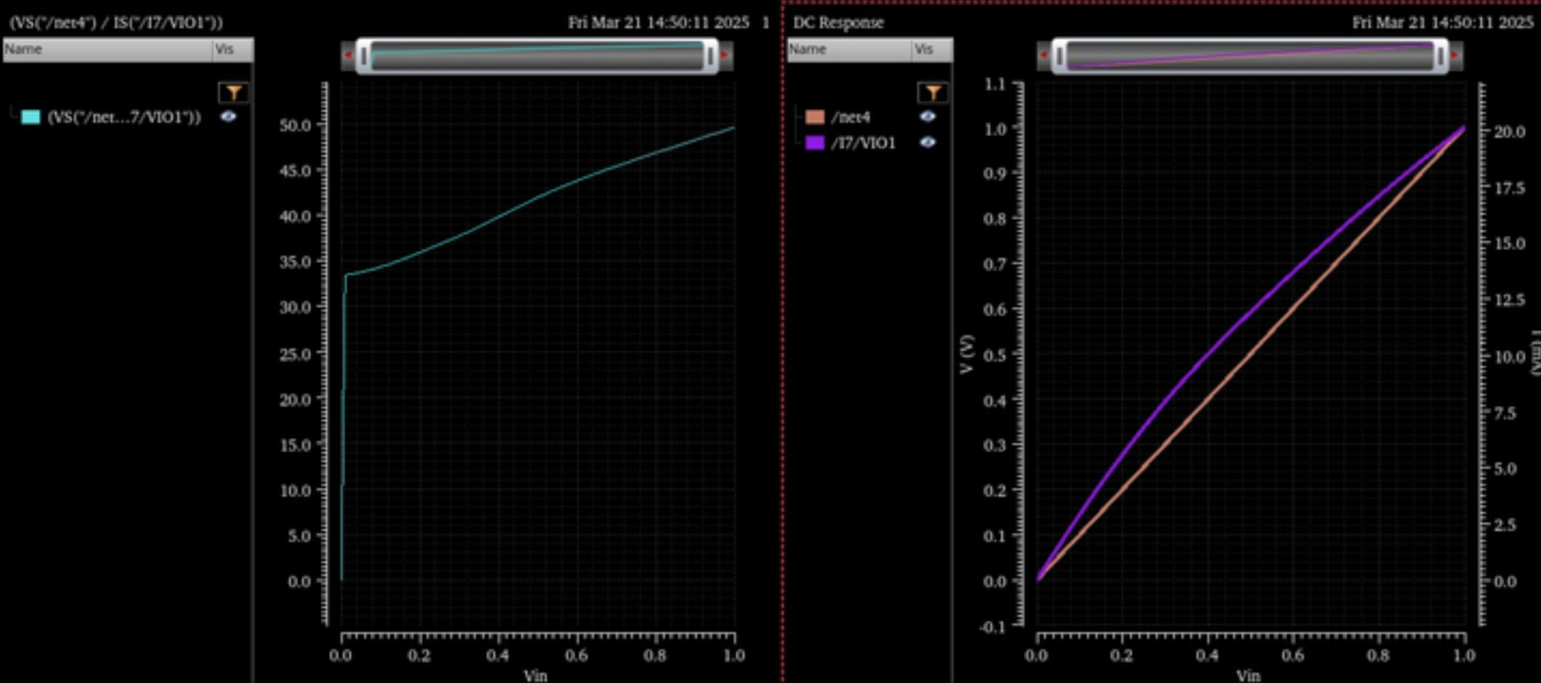
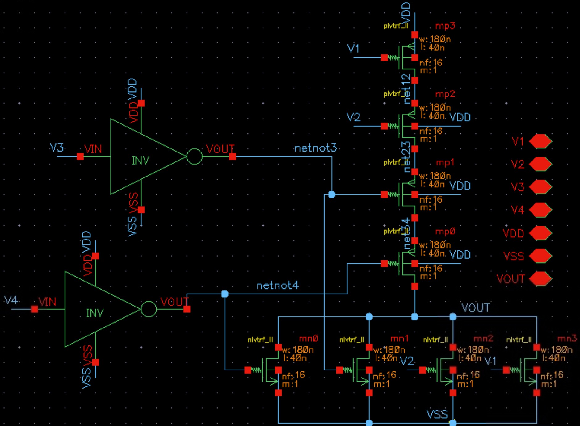
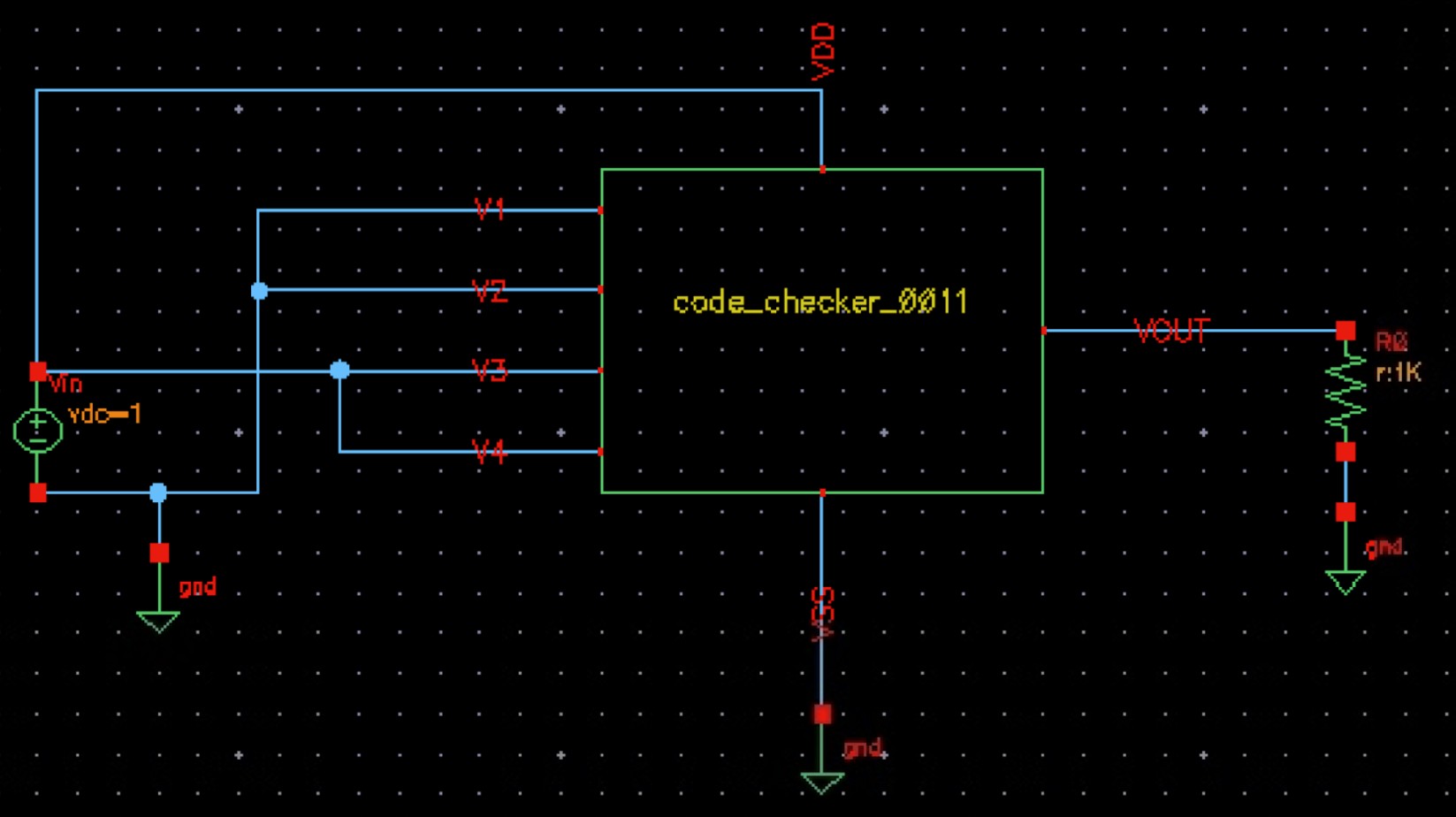
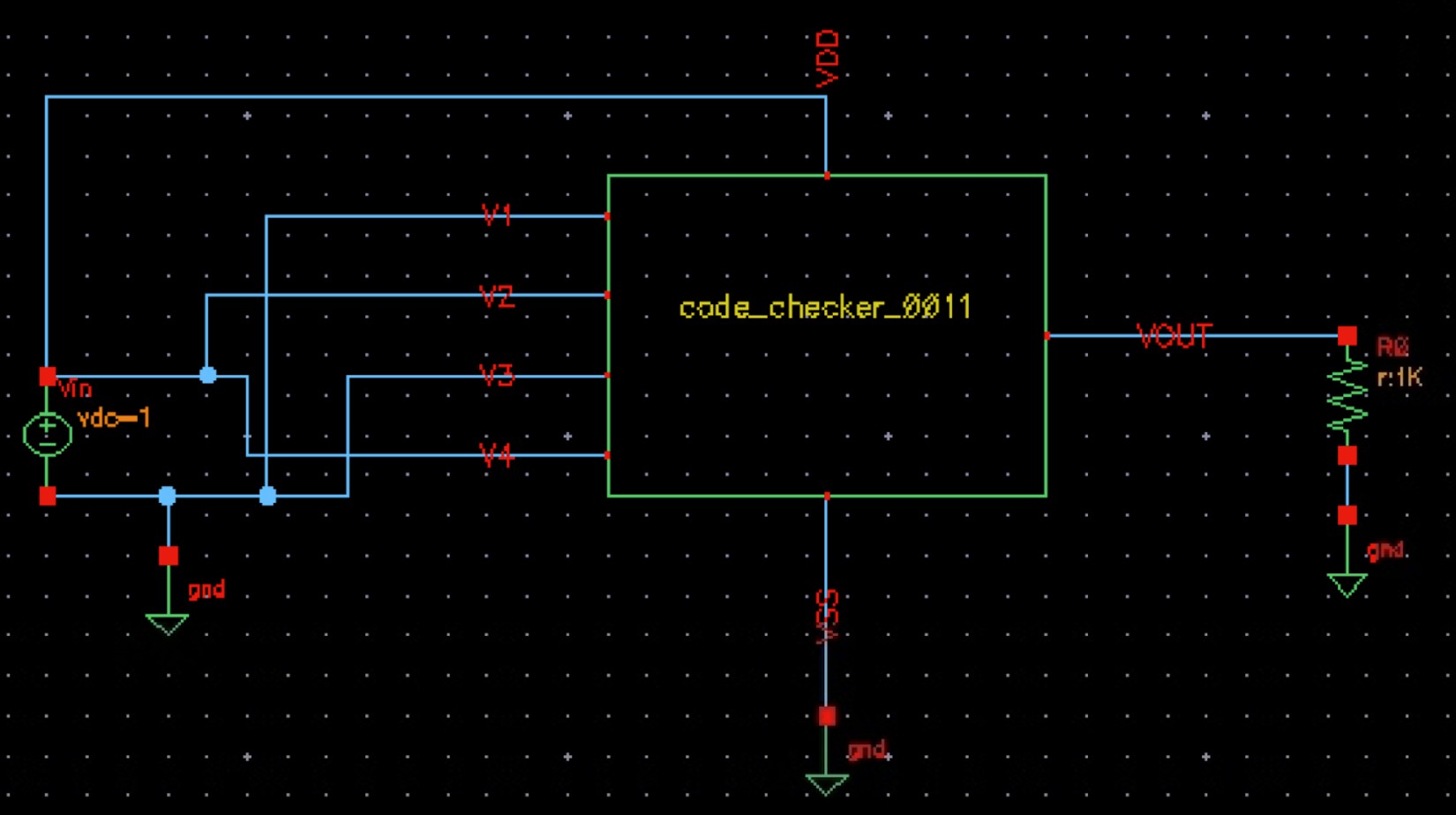
Code Checker
Transistor Sizing:
- mp3: NF = 16
- mp2: NF = 16
- mp1: NF = 16
- mp0: NF = 16
- mn3: NF = 16
- mn2: NF = 16
- mn1: NF = 16
- mn0: NF = 16
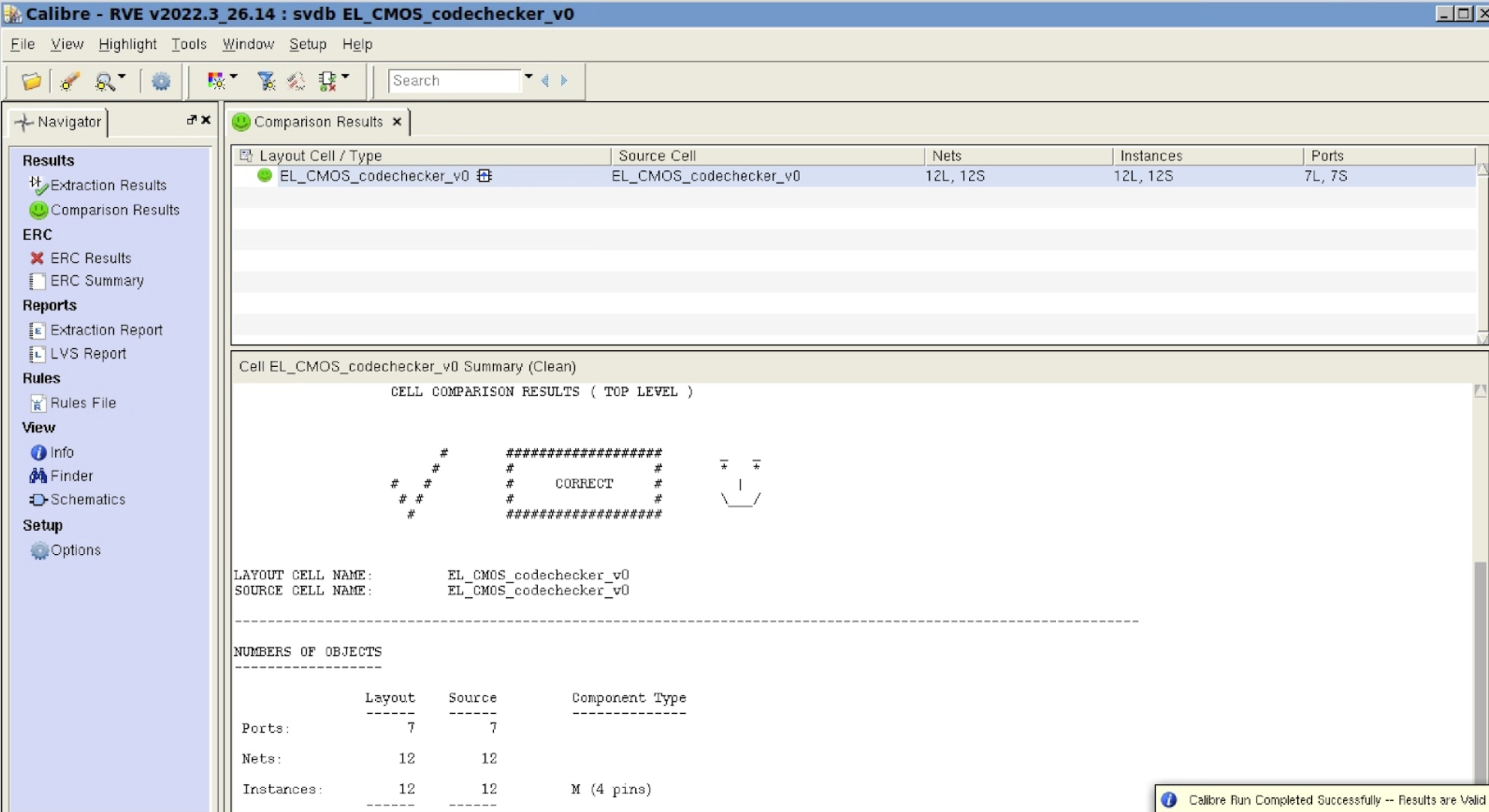
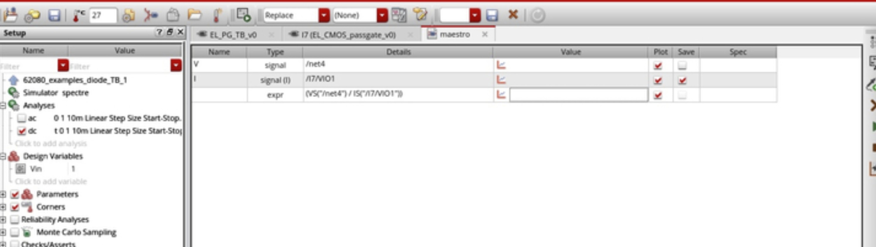
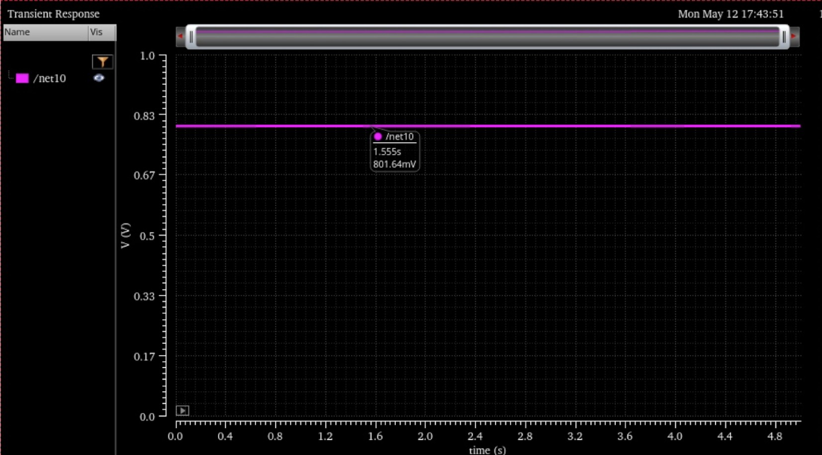
Code Checker Simulation:
With code of 0011, we see a voltage output of around 1V (800mV). I suspect the loss of 200mV is due to resistances of the FETs.
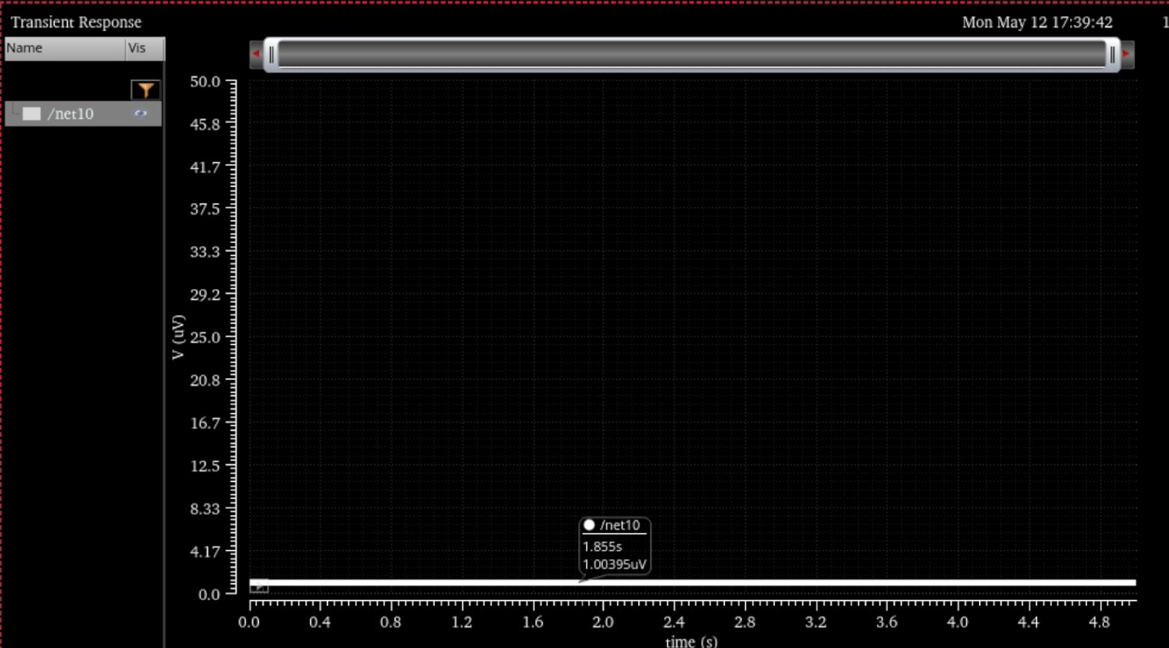
With incorrect code of 0101, we see a low voltage output signal of around 1µV:
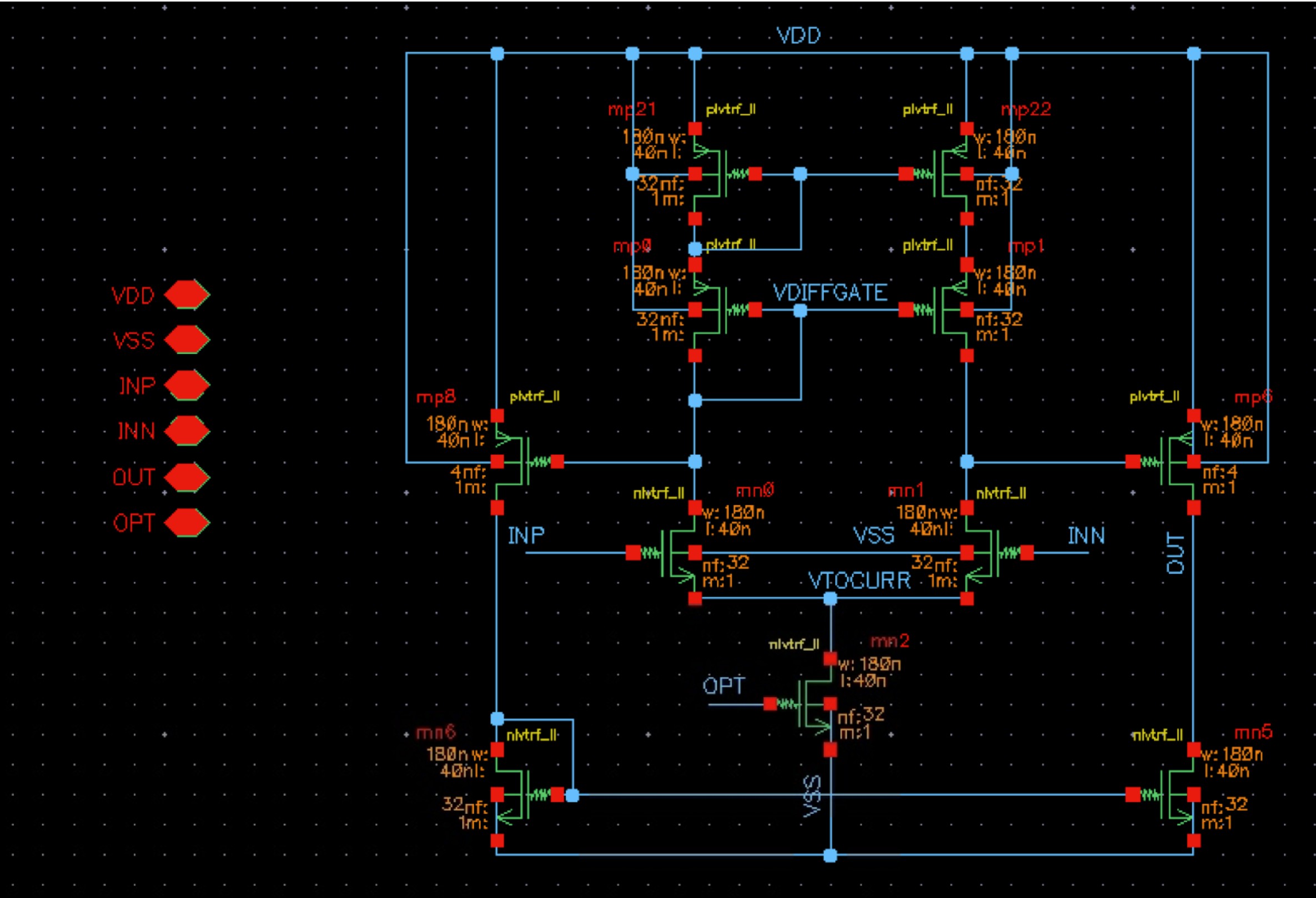
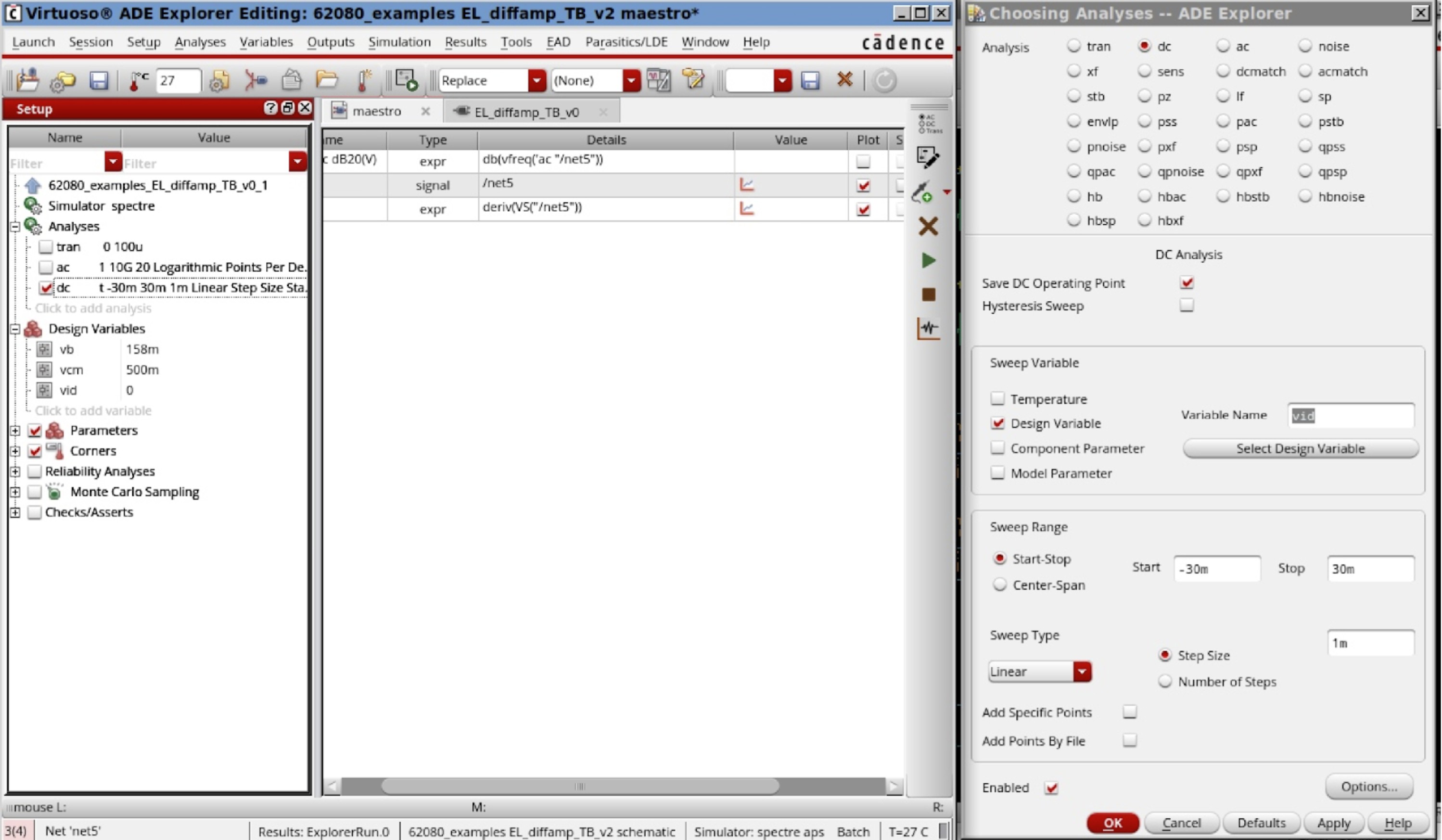
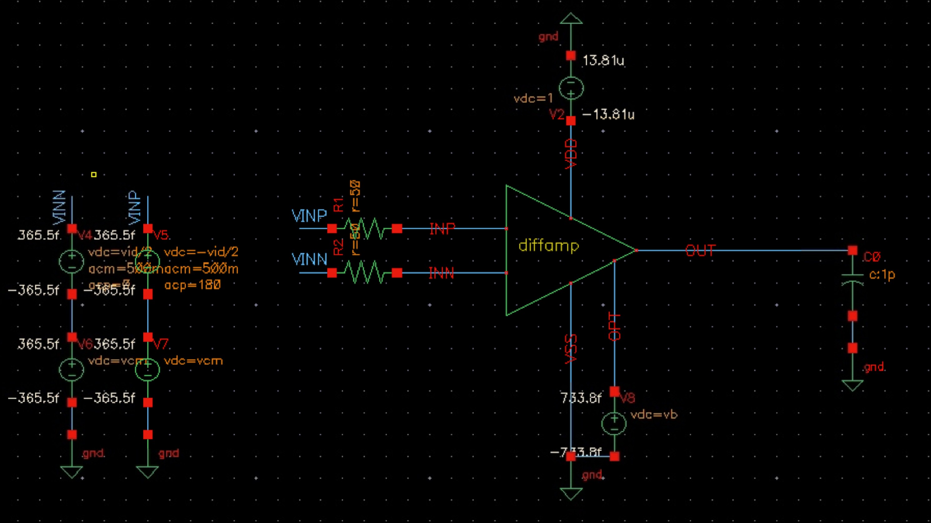
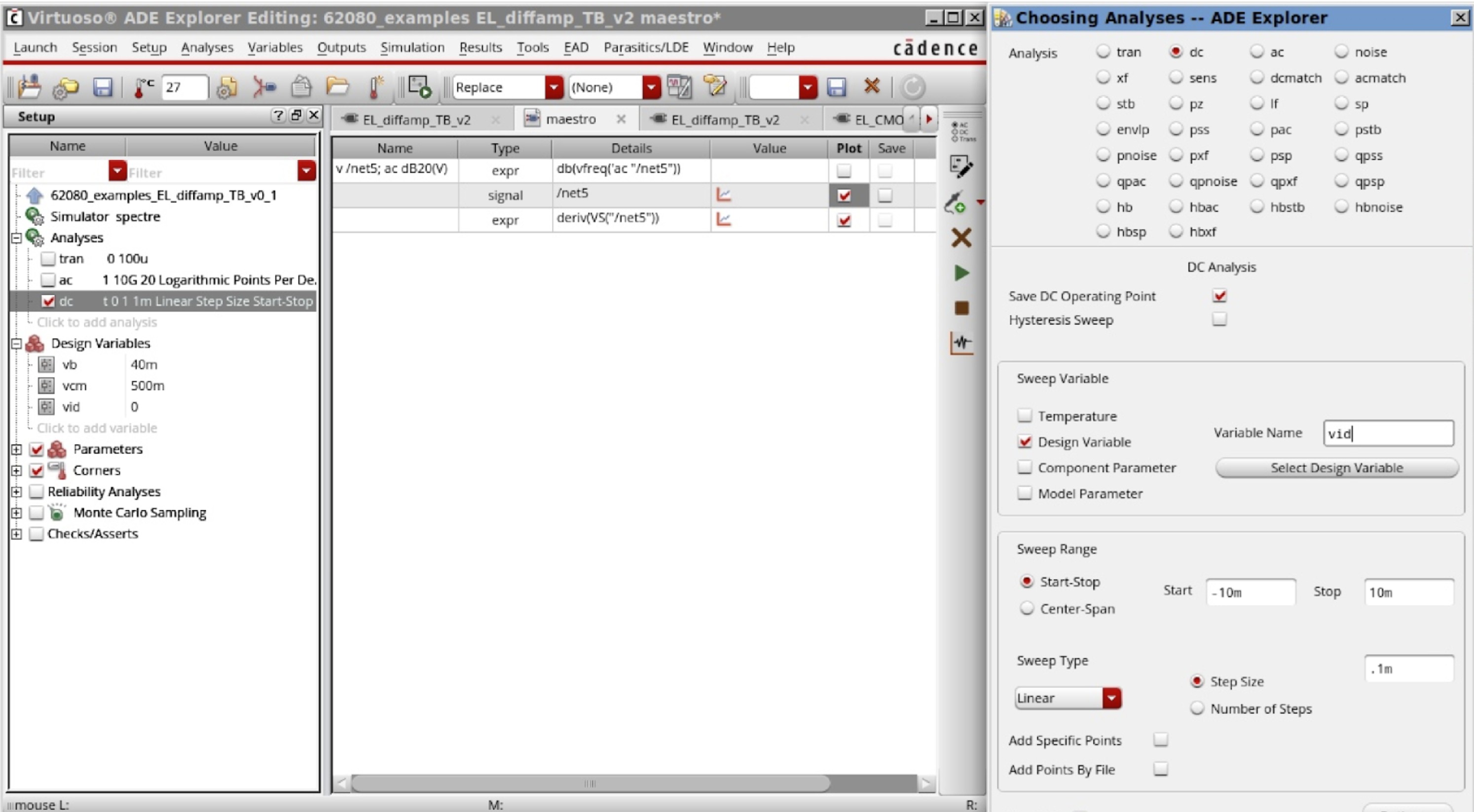
Differential Amplifier
Transistor Sizing:
- mp0: NF = 32
- mp1: NF = 32
- mp6: NF = 4
- mp8: NF = 4
- mp21: NF = 32
- mp22: NF = 32
- mn0: NF = 32
- mn1: NF = 32
- mn2: NF = 32
- mn5: NF = 32
- mn6: nF = 32
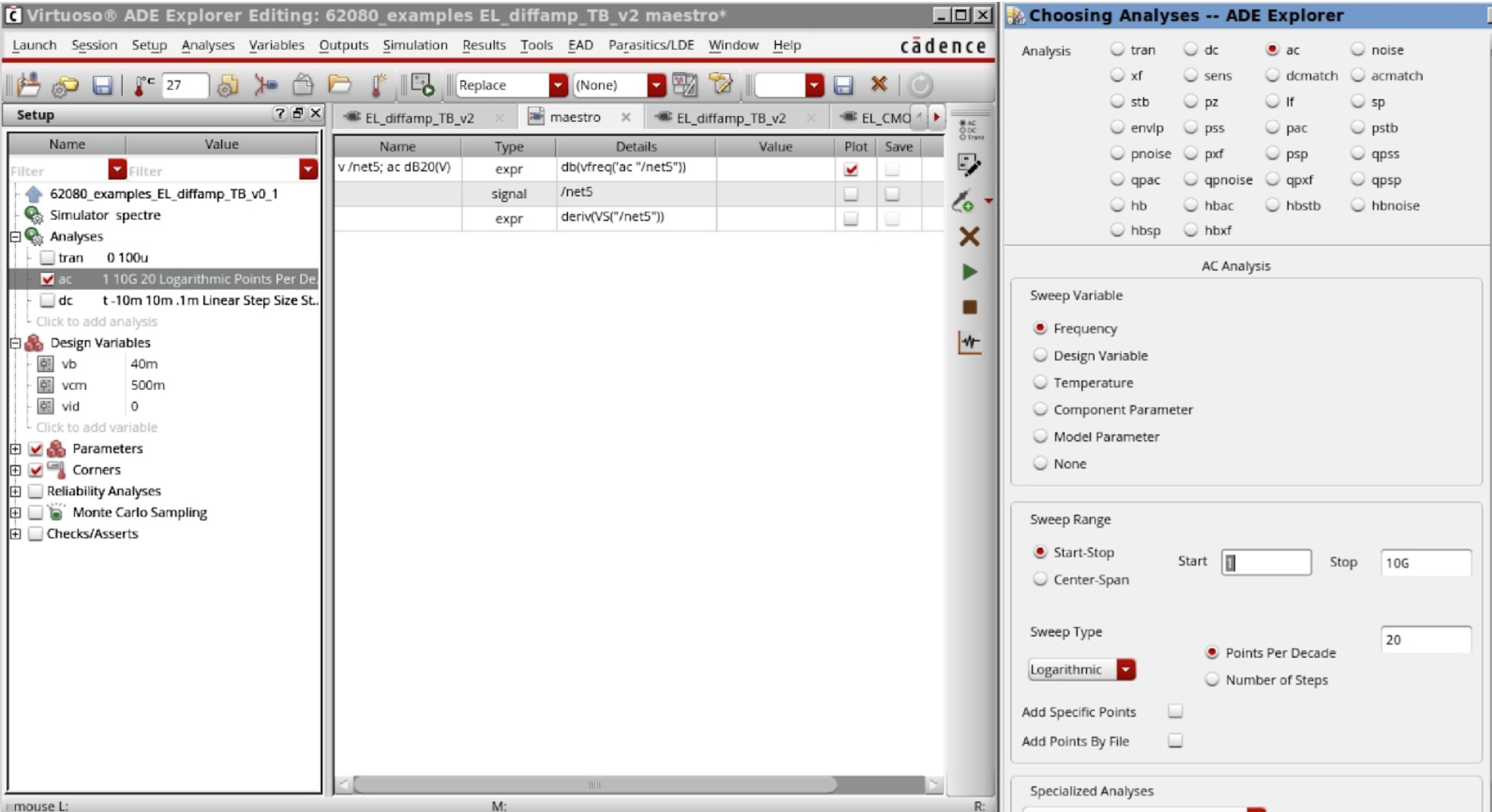
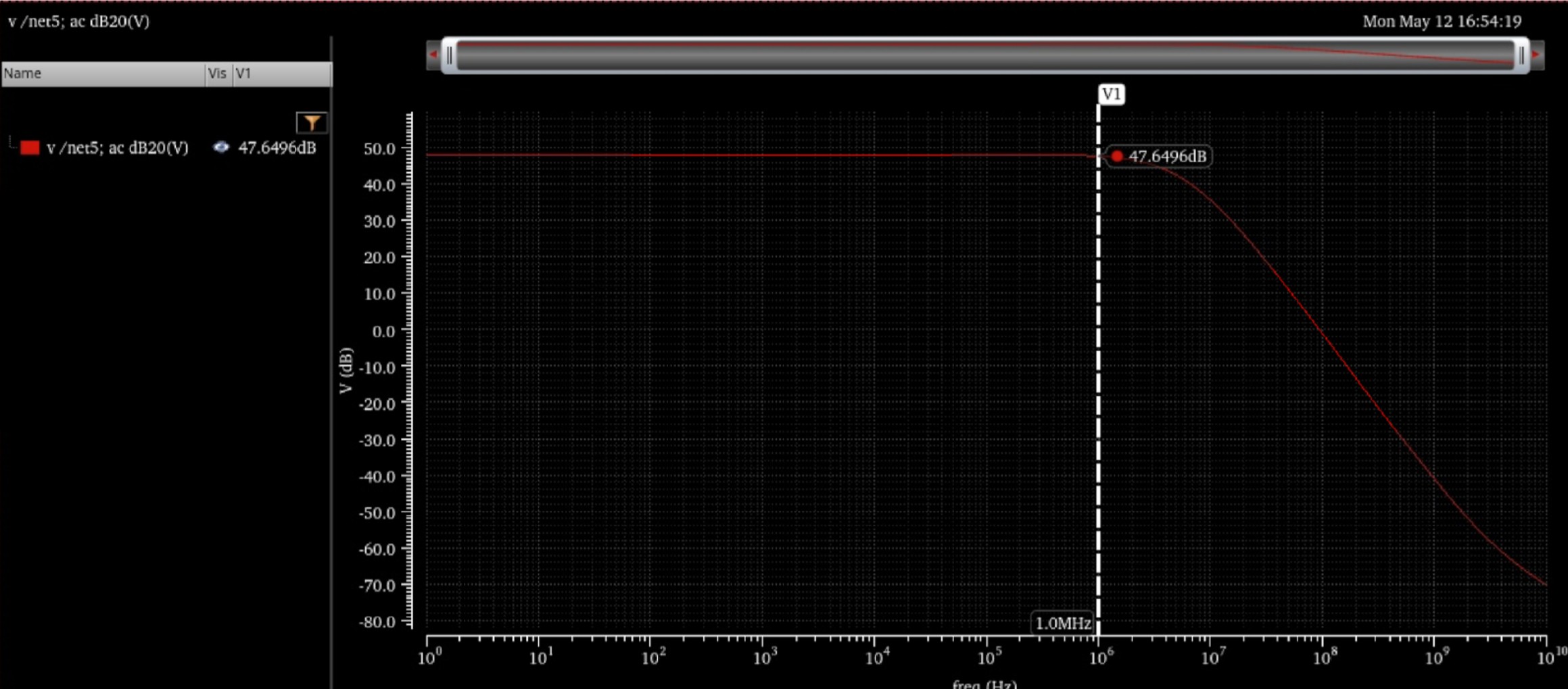
Diff Amp Simulation
Gain:
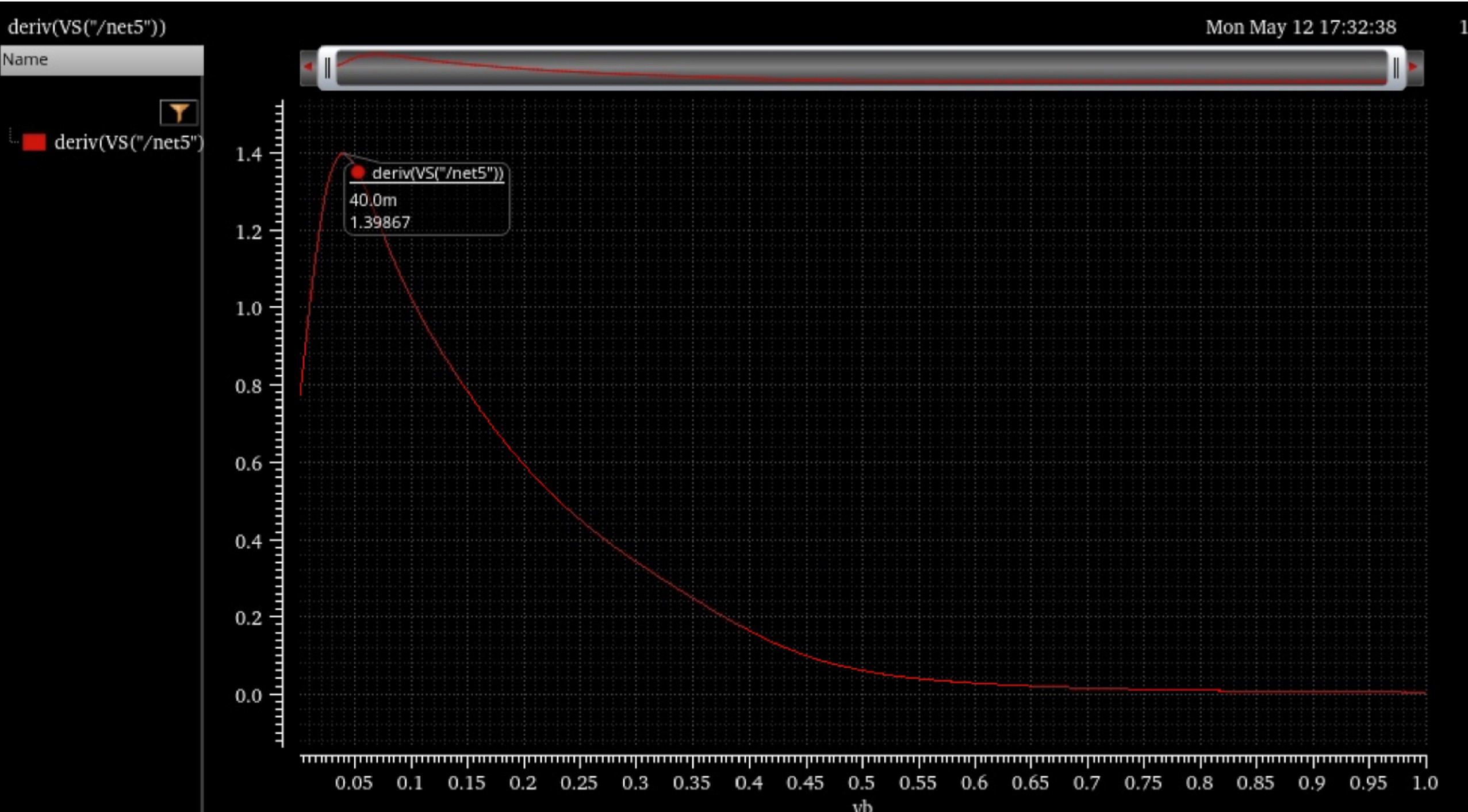
 (Optional Vb swept and found that 40mV was most optimal:)

Power Consumption:
Power consumption: 13.81u * 1V = 13.81uW
Output Swing:
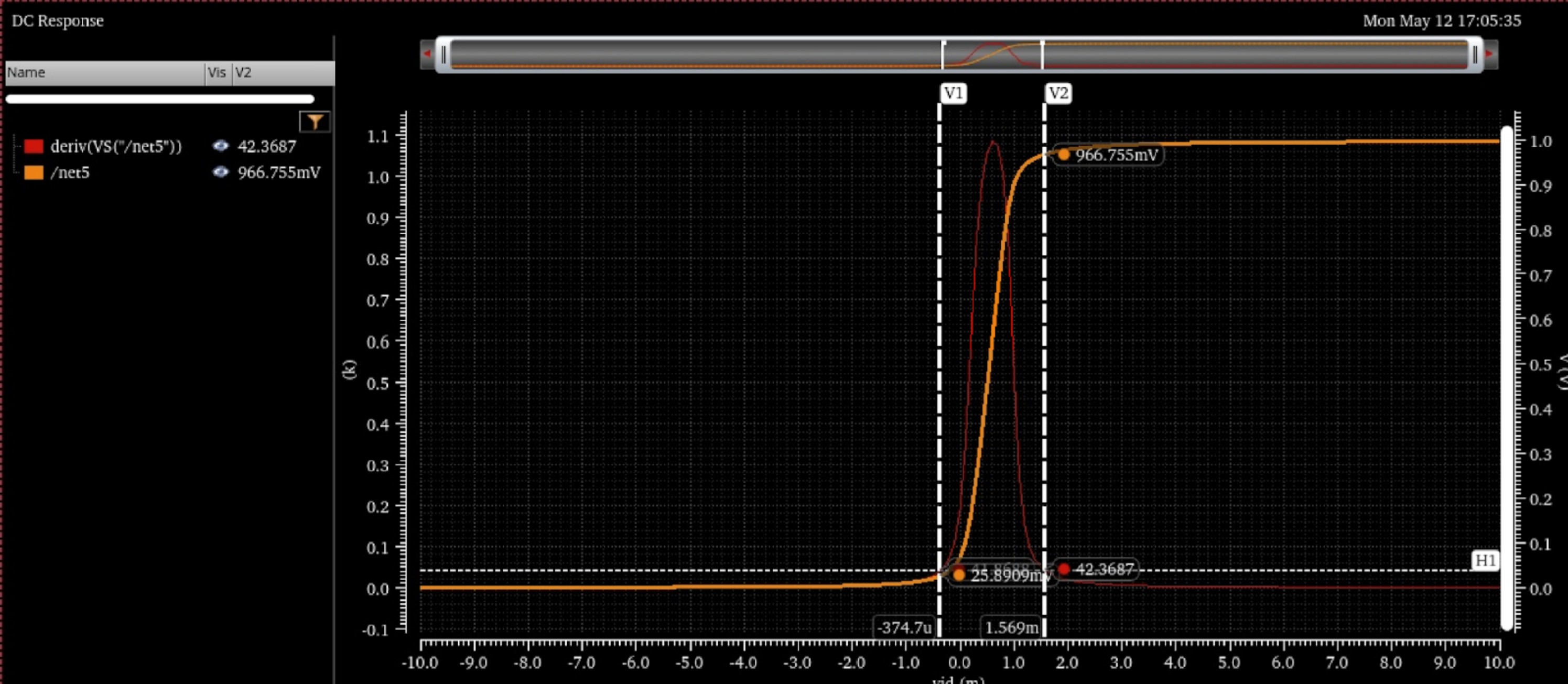 ⇒ 966.755 – 25.8909 = 940.8641mV
Output DC Node Voltages:
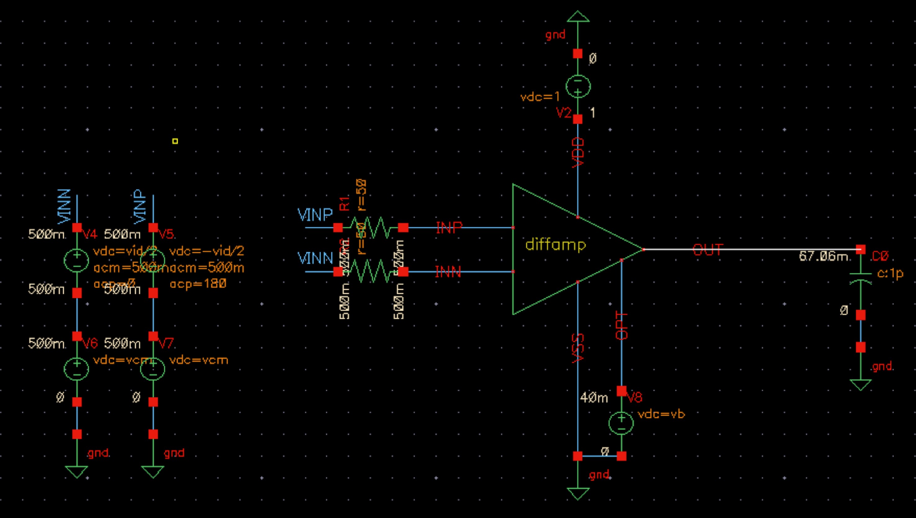
Figure of Merit:
[ 47.649dB * 940.86mW] / 13.81µW] = 3246.27 V/mW